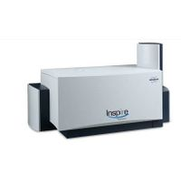
Bruker Corporation - Inspire
Provices the highest-resolution nanoscale chemical and property mapping combined with radical productivity advances and uncompromised AFM performance
Taking full advantage of Bruker’s exclusive PeakForce Tapping® technology, Inspire’s new approach to infrared scattering scanning near-field optical microscopy (sSNOM) extends its capability to nanoscale chemical mapping of a wide variety of samples. The new technique, PeakForce IR™, interleaves sSNOM signal acquisition with PeakForce Tapping feedback, providing the full combined set of information at the same time.
Active Questions & AnswersAsk a Question
There are no current Discussions
Need Equipment Support?
Documents & ManualsView All Documents
Features of Inspire
Highest Resolution Chemical Mapping with sSNOM
Spatio-spectral chemical imaging in polymers * Plasmonics probing in the 2D electron gas of graphene * Material type identification: metals vs semiconductors vs insulators * Film thickness variation with molecular monolayer sensitivity
Chemical Imaging for New Materials * Powders and polymer brushes where neither contact nor TappingMode succeed * Rubbery components, metals, semiconductors, ceramics, and other samples not conducive to photothermal approaches * Samples not microtomable into thin slice or not mountable onto hydrophobic support * Samples that don’t reflect, transmit, or are not Raman active
Highest Resolution Correlated Properties Mapping * Modulus, adhesion, deformation, and AFM topography images with up to atomic defect resolution * Previously unattainable conductivity and workfunction mapping with high resolution even on soft and fragile samples
A new level of productivity * High-resolution infrared imaging with scan rates of up to 10Hz * Fast optical setup of the integrated optics with point-and-click optical alignment guided by an optical field map * Easier, faster, more consistent AFM imaging with Bruker’s proprietary ScanAsyst® automatic image optimization
General Specifications
| Microscope Type | Atomic Force |
Additional Specifications
Optics
Integrated infrared scattering SNOM system:
Includes all required optics, laser, and detector;
High-quality broadband optical components;
Lowest-noise, liquid N2-cooled detector;
Accurate interferometer control;
Low-noise Quantum Cascade Laser source;
Optimized near-field collection and excitation optics
AFM Head Application module-ready AFM head (supports all optional modes)
Scanners
125Μm x 125Μm X-Y x 5Μm Z range;
Other scanner options available upon request
Controller
NanoScope® V Control Station with v9.0 NanoScope real-time control software;
NanoScope v1.5 analysis software;
Windows 7 Operating System
Modes
Scanning probe IR modes:
IR sSNOM operated in TappingMode™ and PeakForce IR™ mode
General imaging modes:
ScanAsyst® Torsional Resonance Mode
PeakForce Tapping® Scanning Tunneling Microscopy
TappingMode Lateral Force Microscopy
Contact Mode PhaseImaging™
Optional material characterization modes:
PeakForce KPFM™ Nanoscale Thermal Analysis
Conductive AFM Liquid Imaging
PeakForce TUNA™ Electrochemical SPM
PeakForce QNM® Nanoindentation
PeakForce Capture™ Piezo Force Microscopy
Force Volume Electric and Magnetic Force Microscopy

